

Introduction
Last year around mid-September, just a few days before the deadline, I found out about a great opportunity from a senior. This was the NXP WIT Scholarship and Mentorship Program 2022, launched for the first time to nurture women leaders in the semiconductor and VLSI field in India.
My keen interest in the ongoing expansion of the semiconductor industry in India, along with the commendable efforts of the government to support its growth, had kept me engaged for quite some time. The world of semiconductors and VLSI held a particular fascination for me, and it was this curiosity that led me to apply to this program.
I eagerly filled out the registration form, recognizing the potential this program had to advance my journey in this ever-evolving field. The prospect of gaining deeper insights into semiconductors and VLSI, combined with the promise of mentorship, was too enticing to pass up. This decision marked a pivotal moment in my quest to delve deeper into a realm I've long been curious about.
Eligibility
Last year, the students pursuing B.E. / B.Tech. who had completed their first year and graduating in 2025 from electronics, computer science and other related engineering courses were eligible to apply to this program. The program’s maximum intake was 50 students and would last a year for them.
Selection Process
The selection process was structured around three progressive stages, each being eliminative in nature. Let me break down each stage for you:
Stage 1: Shortlisting
In the initial stage, the selection process commenced with a shortlisting round, where around 500 students were chosen from a pool of over 5000 applicants. These selected students were then invited to participate in the subsequent aptitude and paragraph writing test. To stand out among other applicants, having a strong academic and co-curricular background, coupled with a genuine interest in technology, electronics, physics, and semiconductors, played a crucial role.
Stage 2: Aptitude and Paragraph Writing Test
The second stage encompassed an aptitude and paragraph writing test. In this one-hour test, we were tasked with responding to approximately 25-30 aptitude questions. Furthermore, we were required to express our enthusiasm for participating in the scholarship and mentorship program through an essay-style question that followed the aptitude section. Following this stage, approximately 150 students progressed to the final stage—the interview round.
To excel in this stage, thorough preparation was paramount. Focusing on logical reasoning, quantitative aptitude, mathematics, and physics-related questions was essential. Moreover, paying special attention to electrical and semiconductor topics within the realm of physics proved to be advantageous.
Stage 3: Interviews
In the final stage, I had to go through a virtual interview. The interview lasted around 45 minutes and included a mix of technical and behavioral questions.
Drawing from my own experience, I realized the importance of knowing the details listed on my resume well. If you've mentioned topics like Object-Oriented Programming (OOP) or machine learning, expect related questions. Similarly, questions about circuits might come up. On the behavioral side, be ready to answer questions like: Why are you interested in this scholarship program? What appeals to you about semiconductors and technology? How do you think you're a suitable candidate for this program? Situational questions might also be posed.
Remember, your preparation and ability to articulate your interests and experiences clearly can significantly enhance your performance across all three stages.
Selection and Perks
Finally, the moment arrived on October 31, 2022, when I received an email that conveyed my selection for the NXP WIT Scholarship and Mentorship Program 2022. My joy knew no bounds on that day. Being one of the top 50 students chosen for the first-ever batch of this scholarship and mentorship program was truly a source of immense delight for me.
Being a part of this program granted me access to a wide array of valuable perks and benefits that truly enriched my experience:
A year-long series of technical classes led by industry experts, aimed at nurturing innovation.
A balanced curriculum that intertwines practical sessions directly relevant to the industry with essential theoretical knowledge.
The exciting opportunity to earn a monetary reward of INR 50,000 upon successful completion of the WIT program.
Preferential consideration for internship and job opportunities at NXP, basis on eligibility.
The privilege to build meaningful connections with mentors specializing in silicon technology.
A student-friendly schedule meticulously designed for convenience, allowing me to engage in learning comfortably from my own home.
These advantages not only contributed to enhancing my skills and knowledge but also unveiled tangible pathways to real-world opportunities within the dynamic semiconductor industry.
My Ongoing Journey in the NXP WIT Program
My journey within this program continues to be both enlightening and enriching. The program spans a year, with a modest commitment of two hours each for three sessions a week. These sessions are meticulously designed to provide us with a comprehensive and industry-ready VLSI curriculum. The real excitement comes alive every Tuesday, as we engage in the special NXP Connect sessions. These sessions offer us a direct link to NXP leaders, allowing us to absorb their insights and learn from their experiences firsthand.
To ensure we're making the most of this opportunity, the program keeps us deeply engaged. Regular assignments and tests are integral components, offering us a chance to put our learning into practical use and assess our progress along the way. This learning experience is all about hands-on engagement and a consistent journey toward growth.
Furthermore, I can't help but emphasize the impact of the knowledge-filled sessions and the bonds I've forged with fellow scholars. These interactions add an invaluable layer to my journey, fostering not only learning but also friendships that are bound to last beyond the program's timeline.
Back in June 2023, something exciting happened – I had the incredible opportunity to visit the NXP India office in Noida and meet the leaders there! This awesome experience was part of a special retreat arranged for us 50 scholars. I've captured all the excitement and details of this amazing adventure in my LinkedIn post. Check it out here: NXP WIT 2022 Retreat
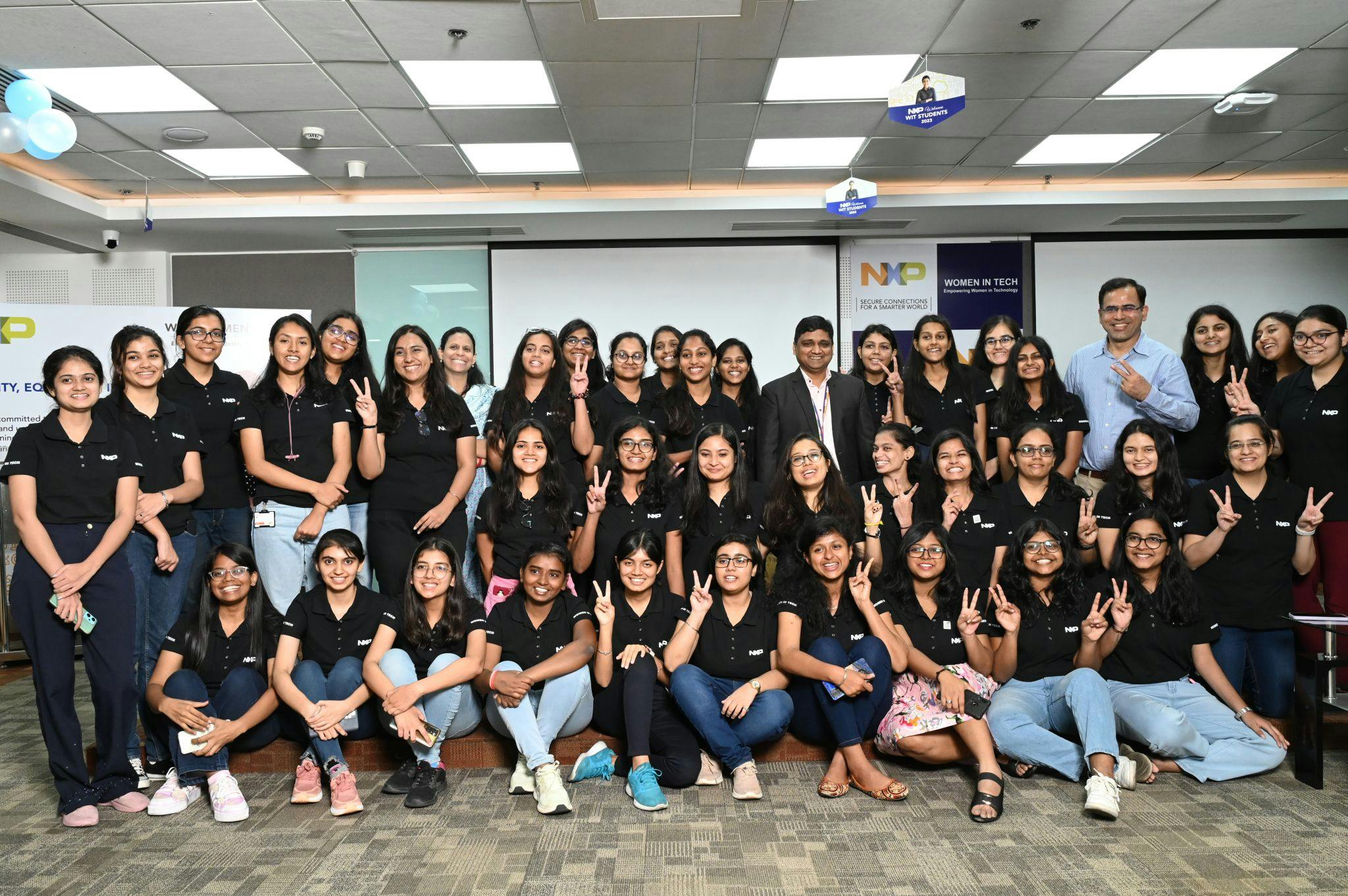
Above is a group picture taken at NXP India's Noida office during the retreat.
Thank you for staying with me through the end of this article. I hope you enjoyed reading it. If you have any questions, please feel free to reach out to me on LinkedIn. You can find me on LinkedIn at ananyagupta05.